
X nano, shorthand for nanoscale engineering, means designing and manipulating materials at dimensions between roughly 1 and 100 nanometers, where a single nanometer is one billionth of a meter. At that scale, materials behave differently. Their optical, electrical, and chemical properties shift in ways that bulk versions of the same substance simply don’t show.
For solar power, that shift is the whole point. Nanotechnology in solar energy uses structures such as quantum dots, nanowires, and thin nanostructured coatings to capture more sunlight, move electrons more efficiently, and cut the amount of material a cell requires. A nanoscale surface texture, for example, can trap light that would otherwise reflect away. Tuning a particle’s size can change which wavelengths of light it absorbs.
This article explains what nanoscale engineering is in plain terms, how it works inside a solar cell step by step, which materials are involved, and where the technology is being applied. We rely on peer-reviewed research and established institutional sources, and we stay with what the evidence supports rather than what the marketing promises.
What Nano Means for Solar Cells

Why Conventional Solar Cells Leave Energy on the Table
A standard silicon solar cell is a single-junction device, and that design carries a built-in ceiling. The Shockley, Queisser single-junction limit puts the maximum efficiency of a cell with one band gap at roughly 30 percent under standard sunlight. Real silicon panels fall short of even that, and the gap comes from losses at nearly every step.
Start with the physics of the band gap. Photons carrying less energy than silicon’s band gap pass straight through without being absorbed. Photons carrying more energy than the band gap are absorbed, but the surplus is shed as heat within picoseconds. Both effects waste part of the solar spectrum before any current flows.
Then come the practical losses. Flat silicon surfaces reflect a meaningful share of incoming light, which is why manufacturers add anti-reflective coatings. Inside the cell, electrons and holes can recombine before reaching the electrodes, and the thicker the absorber, the longer that journey becomes.
These are the pressure points nanotechnology targets. Better light capture, tunable absorption, and shorter charge paths each address a specific loss, as the next sections explain.
How Nanotechnology Works Inside a Solar Cell
Trapping and Tuning Light
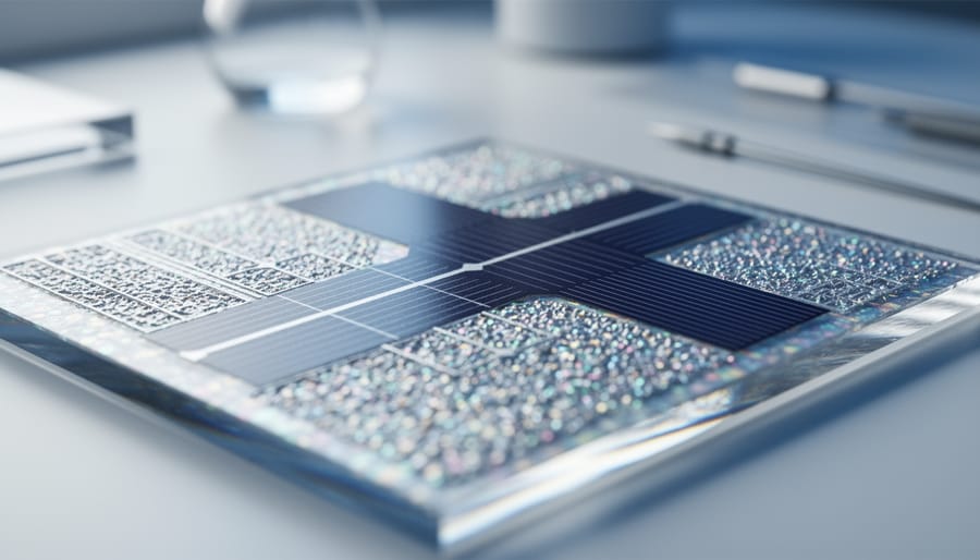
Light that reflects off a panel or passes straight through it produces no electricity, so much of the work at the nanoscale comes down to catching more of it. Anti-reflective nanotextures do this by etching or coating the surface with features smaller than the wavelength of light. Instead of meeting an abrupt boundary where it can bounce back, incoming light sees a gradual change in density, much like the moth-eye pattern in nature, and more of it enters the cell.
Plasmonic nanoparticles tackle a different problem. Tiny metal particles, typically gold or silver, make electrons at their surface oscillate in response to light. That resonance can scatter light sideways inside a thin absorber layer, forcing it to travel farther and giving the material more chances to absorb it. This matters most in thin-film cells, where the active layer is too slim to capture much on a single pass.
Quantum dots address the spectrum itself. Because their size sets which wavelengths they absorb, a single material can be tuned across the visible and into the infrared by changing particle diameter alone. Research into quantum nanotechnology explores how layering dots of different sizes could harvest light that conventional silicon wastes, particularly the lower-energy infrared portion of sunlight.
Moving Charge More Efficiently
In a conventional thick absorber, an electron freed by sunlight may have to travel a long, winding route to reach an electrode. Along the way it can meet a defect or a “hole” (the positive charge left behind) and recombine, releasing its energy as heat instead of electricity. Nanostructures attack this problem by shortening the trip.
Nanowires and nanotubes act like tiny one-dimensional highways. Because their narrow, elongated shape guides electrons along a single direction, carriers reach the electrode with fewer detours. Arrays of vertical nanowires also let light absorption run along the wire’s length while charge is collected across its short width, so the two jobs no longer compete.
Nanostructured interfaces help too. Where two materials meet at a finely patterned boundary, the contact area grows and the distance to the nearest junction shrinks. Electrons separate faster and have less time to recombine.
The trade-off is that more interface also means more surface where defects can form, so manufacturing quality matters.
Main Types of Nanomaterials Used in Solar Technology
Quantum Dots and Perovskite Nanocrystals

Quantum dots and perovskite nanocrystals are tiny semiconductor crystals, often just a few nanometers across, whose size controls the color of light they absorb and emit. Make the crystal smaller and it absorbs shorter wavelengths; make it larger and it reaches further into the infrared. That tunability lets researchers match a absorber layer to different parts of the solar spectrum, which is why these materials are attractive for thin-film cells and for tandem designs that stack layers to capture more sunlight than a single silicon junction can.
Perovskite nanocrystals add easy solution-based processing, which could lower manufacturing cost in principle. The open questions are practical ones. Many perovskites degrade when exposed to moisture, heat, and prolonged light. Leading lead-based compositions also raise toxicity concerns, so researchers are testing encapsulation methods and lead-free alternatives. Both challenges remain active areas of study, and results from the laboratory do not yet guarantee long outdoor lifetimes.
Nanowires, Nanotubes, and Plasmonic Structures
Not every nanomaterial in a solar cell absorbs light. Nanowires, nanotubes, and plasmonic structures mostly work as supporting architecture, shaping how light travels and how charge moves, while another material does the absorbing.
Semiconductor nanowires, for example, can stand upright like a dense forest. Light bounces between them and gets trapped instead of reflecting away, and each wire gives electrons a short, direct route to the electrode. Carbon nanotubes serve a similar role as highly conductive pathways, and researchers also test them as transparent electrodes.
Plasmonic structures take a different approach. Metal nanoparticles, typically gold or silver, concentrate light into a thin absorbing layer at specific wavelengths, which helps thinner cells capture more sunlight.
The contrast with quantum dots is useful. Quantum dots change which wavelengths a material absorbs. These structures change where light goes and how efficiently charge escapes. Most of this work remains at the laboratory stage, and results vary widely with design and fabrication quality.
Where Solar Nanotechnology Is Used Today
Nanoscale engineering already shows up in several parts of the solar sector, though the maturity varies a lot. Anti-reflective and self-cleaning coatings are the clearest commercial success. Nanoporous silica layers, for instance, reduce glare and keep more light entering the glass, and they now appear on many panels sold for rooftops and utility sites, including the kind of home solar power solutions that homeowners compare today. Perovskite and quantum dot cells sit at the other end, where most of the evidence comes from research labs.
Here is how the main applications stack up:
- Anti-reflective nanocoatings on panel glass: commercial, widely deployed.
- Self-cleaning hydrophobic or photocatalytic coatings: commercial, with performance depending on climate and dust type.
- Perovskite-on-silicon tandem cells: pilot and early commercial lines, with durability still under study.
- Quantum dot solar cells: laboratory, with certified efficiencies reported by groups such as those tracked by the U.S. National Renewable Energy Laboratory (NREL).
- Transparent and building-integrated photovoltaics: pilot installations, mostly demonstration projects on windows and facades.
- Flexible and lightweight modules: niche commercial uses, with nanostructured thin films still largely experimental.
- Solar-driven water splitting for hydrogen: laboratory, using nanostructured photoelectrodes.
NREL’s public efficiency chart is a useful reference here, since it lists independently confirmed record cells by technology and shows how far newer nanomaterial designs have come compared with established silicon.
Note the gap between lab records and shipped products. A cell that hits a high efficiency in a small, carefully controlled test doesn’t automatically survive years of heat, humidity, and ultraviolet exposure on a roof. That is why coatings, which improve an already proven product, have reached the market first, while new absorber materials are moving more slowly through pilot lines and field testing.
Expert Perspective on Challenges and Open Questions
Most nanomaterial advances in solar are proven in small, carefully controlled laboratory cells. The harder question is what survives contact with a factory floor and twenty-five years of weather.
Researchers working on quantum dots and perovskite nanocrystals tend to raise the same four concerns. Durability comes first, since many light-absorbing nanomaterials degrade under moisture, heat, and ultraviolet exposure faster than silicon does. Scalability follows: a method that produces a high-performing cell the size of a fingernail does not automatically translate into uniform coatings across a full-size module. Manufacturing cost is the third concern, because precise control over particle size and surface chemistry adds process steps, and the savings promised by thin, material-efficient designs can be offset by that complexity.
Safety is the fourth. Some leading nanomaterials contain lead or cadmium, so encapsulation, handling, and end-of-life recycling matter as much as efficiency. Studies of how nanoparticles behave if released into soil or water are still limited, and honest researchers say so. These trade-offs also bear on climate benefit. A technology only contributes to meaningful GHG emissions reductions if its manufacturing footprint stays low and its panels last long enough to repay it.
Evidence on all four fronts is still emerging, and long-term field data for newer nanomaterial cells remains thin. That is why most researchers favor incremental integration, such as nanostructured coatings on proven silicon panels, over wholesale replacement of established designs.
Common Questions About Nanotechnology in Solar Energy
Is nanotechnology already in commercial solar panels?
In limited ways, yes. Nanoscale anti-reflective and self-cleaning coatings are the most established uses. Quantum dot and perovskite nanocrystal cells are mostly still in laboratory and early pilot stages.
Does it make solar cells more efficient?
It can. Nanostructures help cells trap more light and move charge with fewer losses, and some designs aim to capture parts of the spectrum that conventional silicon wastes. Real-world gains depend on the design, and many results are still lab-scale.
Are nanomaterials safe for the environment?
It depends on the material. Some candidates contain lead or cadmium, which raises toxicity and disposal questions that researchers are actively working to address with safer compositions and better encapsulation.
How is it different from standard silicon cells?
Standard cells rely on bulk silicon wafers. Nano-enabled designs engineer features at roughly 1 to 100 nanometers, either layered onto silicon or used in entirely different thin-film architectures.
Cost is the question readers ask most, and it is the hardest to answer honestly. Nanomaterials could cut costs through thinner active layers and simpler low-temperature manufacturing, but durability, scalability, and production yields still have to be proven before those savings reach the market.
Nanotechnology in solar energy comes down to engineering materials at the scale of billionths of a meter, where light and charge behave differently than they do in bulk. At that scale, designers can trap more sunlight, tune which wavelengths a material absorbs, and give electrons shorter routes to the electrodes. That is the thread running through anti-reflective coatings, quantum dots, perovskite nanocrystals, and nanowires alike.
The realistic outlook is mixed but encouraging. Some nanoscale features, such as coatings and textured surfaces, are already in use, while others remain in the lab, waiting on answers about durability, manufacturing cost, and environmental safety. Progress will likely be incremental, driven by evidence rather than hype.
If you want to keep following the science, explore the related solar and materials coverage across Renewable Innovations, and subscribe to our newsletters for new research summaries and expert interviews as they publish.